In this blog, you can acquire the details about the major differences between types of PCB (2 and 4 Layer PCB). First, we can discuss the fundamentals of each layer and select the apt one which suits your project. Gaining information about Printed Circuit Boards and their working process helps to understand 4-layer and 2-layer PCBs efficiently.
What is PCB?

The fundamental Printed Circuit Board encompasses a thin layer of copper coated with an exclusive insulating substance known to be the substrate. The copper layer is partitioned into different conducting lines widely known as circuit traces. Here, everything happens through the chemical inscription process. The components are electrically connected which builds the circuit. Through the soldering, typical components are integrated into the board. It is feasible to possess bare boards & unique prototyping boards that are not tailored for a concerned circuit. In Addition to standard substrates & copper layers, PCB acts as a safeguard coating that preserves the copper layer from deterioration. At the same time, it reduces the feasibility of aggravating solder shorts.
Perceive details about Layers in PCB
In the domain of electrical engineering, layers are described as copper layers on PCB. The Printed Circuit Board is constructed in augmentation of two layers. If you need more than 2-layer for your project in terms of functionality, you have to enhance the layer count additionally and produce a 4-layer board. In case, if your requirement changes to more than 4-layer, then go ahead with a 6-layer board & so on.
Single layer PCB

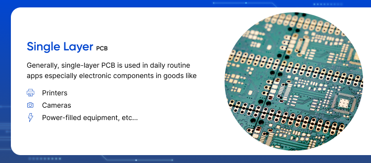
Generally, single-layer PCB is used in daily routine apps. Especially the electronic components in goods like printers, cameras & power-filled equipment, etc. They are the least expensive and most rapid ones when compared to other types of PCBs. Their striking characteristics are simplicity, making them prominent for the enormous manufactured items. A single-layer PCB possesses only one conduction layer.
2-layer PCB

Generally, 2-layer PCBs contain two copper layers. These standard boards are popularly known to be dual-sided boards. The double-sided copper layers are integrated typically with the substrate material. The dual PCB can automatically support and connect the components electrically on double sides of the board. The holes are perforated through a standard board and crumpled with copper. This one automatically leads to the connection of the circuit on a single side of the board to the respective circuits on the other side. It is possible to develop top-notch density circuits on a typical board.
4-layer PCB

In a 4-layer PCB, layers are coated with substitute layers of substrates. Both the top-level layer and ground-level layers are known to be signal layers. These layers prevent EMI along with RF elements. At the same time, it provides restoring signal track and diminishes loop resistance along with a minimal impedance power supply.
Multi-layer PCB

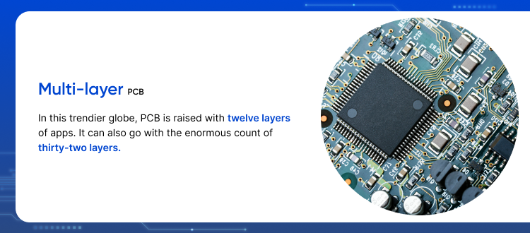
This concerned PCB goes beside four-layer designs. The essential signal layers & pin solidity predicts the layers of PCB. The standard PCB integrated with six layers is used for industrial purposes. Especially machinery, healthcare units, and other technological goods that require refined circuitry. In this trendier globe, PCB is raised with twelve layers of apps. It can also go with the enormous count of thirty-two layers.
Choose between 2 and 4 Layer PCB
In this section, we are going to discuss the unique features of PCB. It helps you to gain details about the board which you are going to implement in your project.
Complexity
The complexity factor decides the number of layers required for your PCB. The complicated circuits possess RF circuitry, a power supply, a digital bus, and other typical components. It is better to use 4-layer printed circuits when compared to other boards. On the usage of a 2-layer board, there will be no emission of radiation. For simple projects of processing circuits, 2-layer PCB is preferred.
Circuit density
Both 2 and 4 Layer PCB provides appropriate space where the components can be integrated on both sides of the boards. The 4-layer PCB holds great functionality.
2-layer Pros & Cons
Pros
Minimal cost
The dual-sided Printed Circuit Boards are the least costly when compared to a 4-layer design. This variance is substantial, relying on the units you needed.
Efficient design
An efficient design is minimally susceptible to costlier issues during the production process. In definite apps, the capability to restore PCB is also essential. When compared to a 4-layer Printed Circuit Board, it is easy to rectify dual-sided PCB.
Large volume
Whenever we need huge production, eradicating inessential layers is important. For projects subjective with large volumes, a 2-layer board is an apt one for the optimization of speed, efficiency & cost.
Cons
Mere design
Typically a 4-layer Printed Circuit Board possesses multiple components & routing choices. On the other side of the flip, 2-layer PCB has a mere design.
Enormous size
The 4-layer PCB possesses multiple layers & double-sided PCB is enormous in comparability to create space for the lead. To fit PCB into compressed space, you have to add several layers. It is one of the finest choices for the design process.
Four Layer Pros & Cons
Pros
Top-notch quality
If a simple product needs high-level quality, then 4-layer PCB is the best choice. If you are ready to pay more, then a 4-layer board is apt. Its main beneficial value is that it offers top-notch quality.
Enhanced power & durability
If you are in need of a 4-layer PCB, then you have to consider. How much power is needed for your design process. For more layers, you have to check the durability of your PCB.
Cons
High cost
The 4-layer PCB is difficult to produce, hence most industrialists prefer 2-layer PCB. If cost is a problem, reducing the level of layers is the best option.
Minimal availability
Nowadays, 4-layer design is a complicated one. It is tedious to explore a manufacturer who can satisfy your needs.
End note!!
From the above points, it is clear that 2 and 4 Layer PCB offers a varied level of functionality. Selecting a 2-layer PCB or 4-layer depends on your project’s requirements, the complexity of the circuit, and the estimated budget.
One of the main factors of using 2 and 4 Layer PCB for IOT product development. Like Smart Water Management solution using IOT and some more IOT devices. Without 2 and 4 Layer PCB IOT products cannot be developed.


